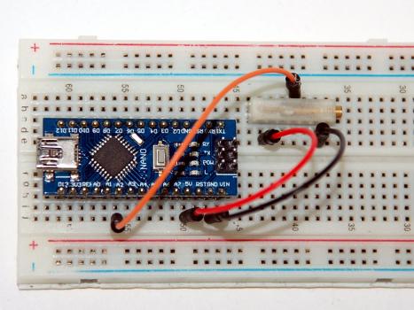
Arduino Nano Analog to Digital Converter
Embedded
10 bit successive approximation ADC (Analog to Digital Converter):
- Converts a continuous analog waveform into a discrete digital representation
- Connected to an 8-channel Analog Multiplexer
- Convert analog input to 10 bit digital values (2^10 = 1024 steps) presented in the Data Register
- Min. value GND (0V), max. value reference voltage AREF
- The ADC has its own interrupt triggering when a conversion completes

Arduino Analog Read
The Arduino function analogRead() reads an analog input signal from pins A[5:0]:
// read analog signal from pin A2
int value = analogRead(A2);
// convert into an 8-bit value
int value = map(value,0,1023,0,255);
The return value has 10-bit resolution, with value from 0 up to 1023.
AVR Analog Read
ADCSRA (ADC Control and Status Register):
| Bit | Name | Description |
|---|---|---|
| 7 | ADEN | Enable (PORTA will behave as GPIO pins) |
| 6 | ADSC | Start Conversion (1 as long as conversion in progress) |
| 5 | ADATE | Auto Trigger Enable (triggered automatically at every rising edge of clock pulse) |
| 4 | ADIF | Interrupt Flag (1 after conversion finished) |
| 3 | ADIE | Interrupt Enable (1 to use interrupt-driven ADC) |
| 2:0 | ADPS[2:0] | Prescale select bits |
// Enable ADC
ADCSRA |= (1<<ADEN);
// Start single analog to digital conversions
ADCSRA |= (1<<ADSC);
ADPS[2:0] (ADC Prescaler):
- The approximation circuitry requires an input clock frequency between 50kHz to 200kHz
- Frequency division factor produces the desired frequency from the CPU (order of MHz)
- Trade-off between frequency and accuracy
| ADPS[2:0] | Division Factor |
|---|---|
| 000 | 2 |
| 001 | 2 |
| 010 | 4 |
| 011 | 8 |
| 100 | 16 |
| 101 | 32 |
| 110 | 64 |
| 111 | 128 |
// Set ADC prescale sample rate @ 16MHz
ADCSRA |= (1<<ADPS2) | (1<<ADPS1) | (1<<ADPS0); // 16000000/128 = 125Khz
// Set ADC prescale sample rate @ 1MHz
ADCSRA |= (0<<ADPS2) | (1<<ADPS1) | (1<<ADPS0); // 1000000/8 = 125Khz
SFIOR (Special Function I/O Register):
ADATE=1(in ADCSRA in register)- SFIOR[7:5] determine the trigger source for ADC conversion
Multiplexer Selection
ADMUX (ADC Multiplexer Selection) register:
| Bit | Name | Description |
|---|---|---|
| 7:6 | REFS[1:0] | Reference voltage selection |
| 5 | ADLAR | ADC Left Adjust Result (1’ to left adjust) |
| 4 | RES | Reserved (always 0) |
| 3:0 | MUX[3:0] | Analog input channel and gain selection bits for PA[0:7] |
REFS[1:0] voltage reference selection:
| REFS1 | REFS0 | Description |
|---|---|---|
| 0 | 0 | Connect AREF to external reference voltage source (internal Vref off) |
| 0 | 1 | AVCC (+5V) with external capacitor at AREF pin |
| 1 | 0 | Reserved |
| 1 | 1 | Internal Vref (+2.66V) reference with external capacitor on AREF pin |
MUX[3:0] analog input channel selection:
- Single-ended voltage inputs
PORTA(pinsPA[0:7])
| MUX[3:0] | Input |
|---|---|
| 0000 | ADC0 |
| 0001 | ADC1 |
| 0010 | ADC2 |
| 0011 | ADC3 |
| 0100 | ADC4 |
| 0101 | ADC5 |
| 0110 | ADC6 |
ADMUX |= (1<<REFS0); // Set ADC reference to AVCC
ADMUX |= (1<<ADLAR); // Left adjust ADC result to allow easy 8 bit reading
Data Registers
After ADC conversion is complete the data registers present the result:
- Default right adjusted 10-bit conversion result:
- Results from
0up to1023(2^10 = 1024 steps) - Read
ADC(combinesADCL(ADC Low byte) andADCH(ADC High byte))
- Results from
- Use a left adjusted 8-bit conversion result:
- Results from
0up to254(2^8 = 255 steps) - Set
ADMUX.ADLARto 1, sufficient to readADCH
- Results from
ADC = VIN*1024/VREF(VIN voltage on input pin, VREF voltage reference)
Read a 10-bit conversion result:
// start single analog to digital conversions
ADCSRA |= (1<<ADSC);
// wait for conversion to complete
while(!(ADCSRA & (1<<ADIF)));
// read the conversion result
int value = ADC; // (ADCH<<8)|ADCL
// clear ADIF by writing one to it
ADCSRA |= (1<<ADIF);
Read an 8-bit conversion result:
// left adjust result
ADMUX |= (1<<ADLAR);
// start single analog to digital conversions
ADCSRA |= (1<<ADSC);
// wait for conversion to complete
while(!(ADCSRA & (1<<ADIF)));
// read only the high-byte
int value = ADCH;
// clear ADIF by writing one to it
ADCSRA |= (1<<ADIF);