Electronic Componentes
Passive components are the framework on which electric circuits are build:
- No active control behavior, responds to voltage and current
- Dissipates energy (resistors) or stores/releases energy (capacitor, inductor)
- Do not require a dedicated power supply (“glue” parts of the circuit)
Active components typically require an external power source and actively alter the circuit behavior:
- Transistors perform current amplification in proportion to changes in a small input signal.
- Diodes are considered active due to a nonlinear response to current and voltage.
Component specifications (so-called datasheets) describe limits and ratings:
- Tolerance (in percent), parts with less tolerance usually more expensive
- Precision parts should not be used unless for a specific reason (i.e. high-precision measurement)
- Exceeding the working voltage may deteriorate the components material resulting in failure
- Exceeding the maximum voltage may cause the current of arc across the material
- Power rating is the maximum amount of power can safely dissipate (in from of heat)
Electrostatic Discharge (ESD)
- Occurs when accumulated static charge is suddenly discharged (to ground)
- Can damage solid-state components if not handled/stored carfully
- ESD damaged components fail under stress in operation (after some period of time has elapsed)
Wire
Wires for use on breadboards:
- Solid core wire [Einkerndraht] sold in spools of varying length.
- Pre-cut (stripped) wires in a kit in a few different colors and sizes.
- Male to male per wire with header pins attached
- Avoid: Stranded [Drilldraht], magnet or to thin wires.
22awg (American wire Gauge), 0.6mm is the preferred diameter for the wire.
Accurate wire stripping remove the outer layer of plastic without defecting the underneath wire.
- Preferably use a wire stripper to remove a couple of millimeter plastic.
- Use the corresponding notch on the stripper depending on the wire gauge.
References…
Jumper Wires
Aka jumper leads…
- …three versions…
- …male-to-female (M2F)
- …female-to-female (F2F)
- …male-to-male (M2M) …for breadboards
Resistor
Passive electronic component with a linear current-voltage relationship as stated by Ohm’s law
- Used at any voltage/current combination within its dissipating power rating (aka wattage rating)
- Come in various sizes and package types (through hole with axial lead, and SMD)
- The greater the resistors power, the greater its physical size
Power rating for surface mounted ranges from 0.05W-0.25W, for axial outline from 0.125W-2W.
Color Bands
Through-hole resistors use color codes (aka bands) to indicate resistive value and tolerance using rings that encircle the body of the resistor:
- 4-band system: digit, digit, multiplier, and tolerance
- 5-band system: digit, digit, digit, multiplier, and tolerance
| Color | Digit | Multiplier | Tolerance |
|---|---|---|---|
| Black | 0 | 1 | |
| Brown | 1 | 10 | ± 1% |
| Red | 2 | 100 | ± 2% |
| Orange | 3 | 1,000 | |
| Yellow | 4 | 10,000 | |
| Green | 5 | 100,000 | ± 0.5% |
| Blue | 6 | 1,000,000 | ± 0.25% |
| Violet | 7 | 10,000,000 | ± 0.1% |
| Grey | 8 | ||
| White | 9 | ||
| Gold | 0.1 | ± 5% | |
| Silver | 0.01 | ± 10% | |
| None | ± 20% |
Surface-mounted resistors have letter codes printed on the device:
- First two digits: A single number representing the resistance value
- Third digit: Number of zeros to append after the resistance value
Types
Three terminal variable resistors called Potentiometer:
- In effect a continuously variable voltage divider
- Exist in circular rotary form, or as linear/slider style
LDR (Light Dependent Resistor), aka Photocell photo-sensitive resistor:
- Changes resistance (in ohms) depending on a detected light strength
- Photocells are non-polarized, and resistance decreases in relation to a darker light source
- Cheap LDR CdS (Cadmium-Sulfide) cells are inaccurate and have a high variation
- Only enough to detect basic light changes
Resistive humidity sensor (aka humistor) responds to the amount of moister in gas surrounding it.
Capacitor
A capacitor (dt. Kondensator) is a device that holds electrical charge which discharges after the current stops. The amount of charge that a capacitor can store is measured in farads.
| Quantity | Symbol | Unit | Abbr. |
|---|---|---|---|
| Capacitance | C | Farad | F |
Capacitors are manufactured to accept a defined voltage maximum (rating) before breaking. Like resistors, capacitors have a tolerance with their value.
Types
Ceramic capacitors:
- Physically tiny devices designed to hold small amount of charge.
- Non-polarized
- Charge/discharge quickly, therefore are often used in high-frequency circuits
Electrolytic capacitors:
- Offer increased capacitance, and are physically larger
- Polarized (indicated by a mark/strip on the device)
- Often used to smooth power supply voltages, and provide stability for components drawing high current quickly (prevent dropouts and noise in a circuit).
Values
Conversion chart for farads:
| Prefix | Abbr. | Value |
|---|---|---|
| F | 10⁰ = 1F | |
| Milli | mF | 10⁻³F = 0.001F = 1000uF |
| Micro | uF | 10⁻⁶F = 0.001mF = 1000nF |
| Nano | nF | 10⁻⁹F = 0.001uF = 1000pF |
| Pico | pF | 10⁻¹²F = 0.001nF |
Ceramic
Ceramic capacitors have a numerical code printed on the device (i.e. 104):
- First two digits: Capacitor value in picofarads.
- Third digit: Number of zeros to append after the capacitor value.
| Digits | uf | nf | pf |
|---|---|---|---|
| 108 | 0.1 | ||
| 109 | 1 | ||
| 100 | 0.001 | 10 | |
| 101 | 0.1 | 100 | |
| 102 | 0.001 | 1 | 1000 |
| 472 | 0.004 | 4.7 | 4700 |
| 103 | 0.01 | 10 | |
| 333 | 0.33 | 33 | |
| 104 | 0.1 | 100 | |
| 155 | 0.15 | 150 | |
| 224 | 0.22 | 220 | |
| 105 | 1 | 1000 | |
| 685 | 6.8 | 6800 |
Diode
A Diode is a device passing current in one direction depending on the polarity of the applied voltage.
Diodes have a positive terminal (+) called anode, and a negative terminal (-) called cathode. The arrowhead points against the direction of electron flow. If a positive voltage is present on the anode (forward direction) then the diode is “turned on”, and allows current to flow through. In this mode the diode is forward biased. (Most silicon based diodes required a positive threshold voltage of 0.7V to turn on.)
If the voltage across the diode is negative, means that a negative voltage is present at the anode, then no current will flow (like an open circuit). The diode blocks the flow of current in reverse direction, hence is reverse biased. The peek reverse voltage (PIC), or breakdown voltage specifies the maximum reverse voltage level at which the diodes isolation function will break down and current starts to flow in reverse direction.
The gray ring (stripe mark) on the device indicates the side of the cathode.
Measure Diodes with a Multimeter
Make sure your fingers don’t touch the test points/leads, otherwise the skin resistance will be measured.
- If the resistance is zero in both directions, then the diode is shorted.
- If the resistance is infinite in both directions, then the diode is open.
- If the resistance is infinite in one direction and a small resistance in the other direction (open circuit), then the diode is functional.
Knowing which is the positive lead of the multimeter allows to determine the diodes cathode.
Zener Diode
Designed to conduct in reversed biased mode in a controlled way
- The reverse voltage causing the diode to conduct is called the zener voltage (Vz).
- Vz is determined by the resistivity of the diode junction and ranges between 2.7V up to 200V
- Typical applications are voltage regulators.
LED
Light Emitting Diode…
- Active electronic component that produces light when current flows through a crystal
- Different crystals produce colors like red, yellow, green, blue or white
- 2 leads: Anode (positive) & Cathode (negative)
- Polarised: Connected to a circuit in one direction
- Current needs to flow from anode to cathode (otherwise it dose not illuminate)
- The longer lead (anode) goes to the more positive voltage
- The flat spot on the LED indicates the cathode
- Voltage drop: Within a circuit voltage will change across the LED
- Each color has a characteristic voltage drop, e.g. red ~1.7V
- Each color uses a different semiconductor material to emit light of a specific wavelength
- LEDs are current driven:
- Given the required voltage, the crystal in the LED starts to glow
- Increased current will make LEDs brighter until it is eventually destroyed
- Therefore current needs to be restricted by a resistor
- Applications:
- Illumination in e.g. flashlights, TVs
- Status indication in e.g. battery charger, car back light
- Brightness of an LED is measured in Milli-Candela (MCD), ranges from 10-5000 MCD
RGB LED
A device with three internal LEDs of red, green, and blue (RGB) color
- These LEDs combines three light spectra to create a desired color spectrum.
- The RGB additive color model can be digitally represented with an integer number for each of the three colors.
- The color triplets range from 0 to 255 per channel, the darkest color, black is
255,255,255and the lightest color, white0,0,0.
Transistor
Transistors provide amplification and/or switching capabilities.
- Semiconductor device with three or more elements are called Transistor
- Term derived from TRANSfer and resISTOR
Use-Cases:
- Control the flow of a much larger power/current then a controlling device (e.g. a micro-controller) can handle.
- Isolate different regions of complex circuits
- In small quantities used as simple switches, digital logic, and signal amplification circuits
- In big quantities used in Integrated Circuits (ICs) as part of computer memory, and microprocessors
BJP - Bipolar Junction
Three terminal to connect with a circuit:
| Terminal | Abr. | Description |
|---|---|---|
| Base | B | Controls the flow of the current carrier |
| Emitter | E | Emits current carriers |
| Collector | C | Collects the current carriers |
The voltage applied to base-emitter terminals controls the current at the collector terminal. A small current at the base of the transistor allows for a much larger current across the emitter and collector terminals.
Transistors are built by stacking three different layers of semiconductor material together:
- A Material with extra electrons is called n-type (negative charge)
- A Material with electrons removed is called a p-type
- Transistors are created by stacking an n on top of a p on top of an n (NPN), or p over n over p (PNP)
NPN (Not Pointing iN) transistor
- Positive voltage to the collector and base terminals
- Switched “on” if there is current at the base terminal (high signal)
- If on, current flows from collector to emitter
PNP (Point iN) transistor
- Positive voltage to the emitter and negative voltage to the base terminal
- Switched “on” if there is no current at the base terminal (low signal)
- If on, current flows from emitter to collector
Transistor Component
The flat face with text is the front side…
While the voltage on the transistor base (terminal #1) is below the threshold no current will flow between collector (terminal #3) and emitter (terminal #2). This transistor has a threshold voltage of 1V (at the base) to switch on.
Operation Modes
NPN transistor (flip polarity of > and < signs for an PNP transistor)
| Abr. | Description |
|---|---|
| Vᵇᵉ | Voltage from base to emitter |
| Vᵇᶜ | Voltage from base to collector |
| Vᵗʰ | Threshold voltage required at Vᵇᵉ |
| Mode | State | Description |
|---|---|---|
| Saturation | Vᵉ < Vᵇ, Vᶜ < Vᵇ | The transistor acts like a short circuit between collector and emitter |
| Cut-Off | Vᵉ > Vᵇ, Vᶜ > Vᵇ | The transistor acts like an open circuit: No collector and emitter current |
| Active | Vᶜ > Vᵇ > Vᵉ | Current going into the base pin amplifies current going into the collector and out the emitter |
| Reverse-Active | Vᶜ < Vᵇ < Vᵉ | Like forward-active, but the current flows reverse |
Measure NPN & PNP Transistors
Separate NPN from PNP transistors with an Ohm-meter:
- (Use alligator clamps to connect the probes.)
- Connect the positive probe of the meter to the base, and the negative to the collector. If the meter shows a reading then the transistor is an NPN. (Verify by measuring from base to emitter.)
- Connect the negative probe of the meter to the base, and the positive to the collector. If the meter shows a reading then the transistor is a PNP. (Verify by measuring from base to emitter.)
Assuming it is known if the transistor is NPN or PNP:
- Test the base-collector and base-emitter junctions like a standard diode. If one of the junctions does not behave like a diode then the transistor is bad.
- Check the resistance from collector to the emitter. The transistor is functional if there is an open circuit between collector and emitter.
- Some transistors have a diode from collector to emitter then a high resistance is measured between collector and emitter.
- Darlington transistors have a high reading from base to emitter and may appear as open on a volt-meter.
Darlington
Compound device build from two bipolar transistors:
- Two transistors cascaded to act as single amplifier.
- The current gain is the product of the two transistors, therefore it is much higher than each transistor taken separately.
- Only a small input current is required to switch a large load current.
Used in circuits with motors, relays or other current-hungry components connected to a low-voltage micro-controller. Darlington pairs are available with a current gain of 1000:1 (i.e. switching a 1A load current with a 1mA control current).
- The collectors of the two transistors are connected.
- The emitter of the first transistors drives the base of the second transistor.
Disadvantages:
- High minimum voltage drop between base and emitter when fully saturated. The sum of the two base-emitter voltage drops can be between 0.6V to 1.5V depending on the current. This results in a hotter device requiring a better heat sink.
- Slow switch times as it takes longer for the slave transistor to turn the master transistors.
FET - Field-Effect
Another three terminal semiconductor device to switch and amplify, developed to overcome the limitations of BJT transistors.
Terminals in comparison to BJT transistors:
| BJT | FET |
|---|---|
| Emitter (E) | Source (S) |
| Base (B) | Gate (G) |
| Collector (C) | Drain (D) |
IGFET (Insulated Gate FET) transistors:
- Gate terminal isolated from the main current carrying channel (no current flows into the gate)
- Act like a voltage controlled resistor, current flows through the main channel between drain and source, proportional to the input voltage
- High input impedances (MΩ), draws negligible current from the circuit
- Two types JFET (Junction Field Effect Transistor), and the most commonly used type MOSFET (Metal-Oxide Field-Effect)
Classifications into PMOS (P-channel) or NMOS (N-channel)
- Constructions consists of a resistive semiconductor “channel” carrying the current through the FET
- This main channel may be made out of P-type of an N-type semiconductor material
MOSFET
Two basic forms:
- Depletion Type (normally-on) requires a gate-source voltage to switch off
- Enhancement Type (normally-off) requires a gate-source voltage to switch on
Switching tables according to the gate-source voltage (VGS):
| Type | VGS = +V | VGS = 0V | VGS = -V |
|---|---|---|---|
| NMOS Depletion | on | on | off |
| NMOS Enhancement | on | off | off |
| PMOS Depletion | off | on | on |
| PMOS Enhancement | off | off | on |
Sensors
JoyStick
Analog two-axis sensor with push button function.
- Similar in function to analog joysticks found in gamepads (e.g. Sony PS2).
- Push function actuated when the joystick is pressed.
Connectors:
| Pins | Number | Description |
|---|---|---|
| GND | #1 | Ground 0V |
| +5V | #2 | Power, 5V DC |
| VRx | #3 | Analog X-axis, voltage proportional to x position |
| VRy | #4 | Analog Y-axis, voltage proportional to y position |
| SW | #5 | Digital switch, push button function |
- Directional movement for each axis build with potentiometers (~10kΩ).
- The two potentiometers are mounted with a 90 degree angel and connected to a stick in the middle
- Moving the stick will case the analog signal to vary between 0V and 5V (resting position 2.5V)
- Reading the analog signal with a micro-controller will provide values between 0 and 1023 (resting position 512)
Ultrasonic Sensor
HC-SR04 ultrasonic ranging sensor:
- Determine the distance of an object using ultrasonic sound, hence with a non-contact range detection.
- The device is build with distinct ultrasonic transmitter and receiver modules.
Connectors:
| Pins | Description |
|---|---|
| Vcc | Power +5V DC (15mA) |
| Trig | Trigger (input) |
| Echo | Receiver (output) |
| Gnd | Ground 0V |
Measuring angel 30° with a ranging distance of 2-400cm and a resolution up to 3mm.
DHT11 - Temperature/Humidity
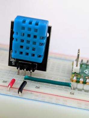
DHT11 temperature and humidity sensor module:
| Pin | Name | Description |
|---|---|---|
| 1 | DATA | I/O port for the micro-controller |
| 2 | VCC | Power +3.3-5V |
| 3 | GND | Ground 0V |
Features:
- …on module 10k Ohm pull up resistor
- …humidity 20-90%RH (+-5%RH), resolution 1%RH
- …temperature 0~50℃ (+-2), resolution 1℃
References…
- DHT11 Datasheet
- Adafruit Arduino DHT library
Serial communication
- Single wire two-way
- DATA pin is high by default
- Start Signal
- Pull down the DATA pin for at leas 18ms to start communication
- Pull up DATA pin for 20-40us to wait DHT11 response
- Response Signal
- DHT11 pulls down data pin for 80us
- Followed by a pull up of 80us
- Transmission Process
- Each bit begins with 50us low-voltage-level
- Ends with high-voltage low-voltage-level
- Length of high-voltage-level signal “0” 26-28us, “1” 70us
Data Transmission
40bit (higher data bit first)
- 8bit integral RH data +
- 8bit decimal RH data +
- 8bit integral T data +
- 8bit decimal T data +
- 8bit check sum.
checksum = 8bit integral RH data
         + 8bit decimal RH data
         + 8bit integral T data
         + 8bit decimal T data
Displays
7-Segment
Display device for decimal numerals 0-9
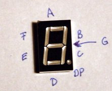
- The seven segments of the display can lit in different combinations to represent numerals
- The digit segments are referred to by letters A-G
- The DP (decimal point) segment is used to display non-integer numbers
Hexadecimal letter digits can be represented with a combination of upper- and lowercase: A,b,C,d,E,F
List of segment states (on/off) to display digits:
| Digit | ABCDEFG |
|---|---|
| 0 | 1111110 |
| 1 | 0110000 |
| 2 | 1101101 |
| 3 | 1111001 |
| 4 | 0110011 |
| 5 | 1011011 |
| 6 | 1011111 |
| 7 | 1110000 |
| 8 | 1111111 |
| 9 | 1110011 |
| A | 1110111 |
| b | 0011111 |
| C | 1001110 |
| d | 0111101 |
| E | 1001111 |
| F | 1000111 |
Terminals for A-G, DP and the common cathode (ground):
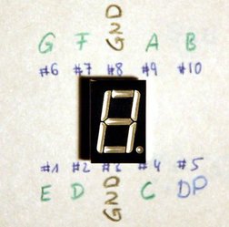
The display uses LEDs, therefore a current-limiting resistor is required!
1602 LCD Module
Display format 16 characters by 2 lines…
- …display font 5x8 dots
- …logic voltage 4.8-5.2V, max 150mA
- …supports 4bit (D4-D7) and 8bit (D0-D7) data operations
- Reference…
| Pin | Name | Description |
|---|---|---|
| #1 | VSS | Ground 0V |
| #2 | VDD | Logic power +5V |
| #3 | VO | Display contrast |
| #4 | RS | Register select (data or instruction register) |
| #5 | RW | Read (high), Write (low) |
| #6 | E | Enable signal for data write or read |
| #7-14 | D0-D7 | 8bit bi-directional data bus |
| #15 | A | Backlight power +5V |
| #16 | K | Backlight ground 0V |
1.5” OLED RGB
Supports 4-wire and 3-wire SPI selected by the BS resistor on the backside
4-wire SPI (Factory setting) BS set to 0:
| Pin | Description |
|---|---|
| VCC | Power 3.3~5V |
| GND | Ground |
| DIN | Data Input, connect to MOSI |
| CLK | Clock Data Input, connect to SCK |
| CS | Chip Selection (low active) |
| DC | 4-wire SPI Data/Command selection (high = data, low = command) |
| RST | Reset (low active) |
Dot matrix OLED controller SSD1351:
- 128x128 screen
128*128*128SRAM display buffer- 265k and 65k gray scale
Usage
Use raspi-config to enable the SPI interface.
Pin wiring:
| Display | Raspberry Pi |
|---|---|
| VCC | 3V3 |
| GND | GND |
| DIN | MOSI |
| CLK | SCK |
| CS | CE0 |
| DC | 24 (BCM) |
| RST | 25 (BCM) |
cd $(mktemp -d)
# install WiringPi
git clone https://github.com/WiringPi/WiringPi
cd WiringPi
git clone https://github.com/WiringPi/WiringPi
cd WiringPi
./build
cd ..
# install BCM 2835 support
wget http://www.airspayce.com/mikem/bcm2835/bcm2835-1.62.tar.gz
tar -xvf bcm2835-1.62.tar.gz
cd bcm2835-1.62
./configure
make
sudo make install
ls /usr/local/lib/libbcm
cd ..
# build the example from Waveshare
git clone https://github.com/waveshare/1.5inch-RGB-OLED-Module
cd 1.5inch-RGB-OLED-Module/c
make
sudo apt install -y \
python3-dev \
python3-rpi.gpio \
python3-smbus\
python3-serial \
python3-spidev